Over the last few decades, silicon wafers are evolving with tremendous change. From undifferentiated commodities to extraordinary products, this has become an obligatory use for keeping up the pace with modern innovations of semiconductor and industry. The supply of bulk wafers is paving a wide path for manufacturers to produce advanced materials and sophisticated substrates like SOI (Silicon-On-Insulator).
Probably, other reasons for efficient production of wafers is to help Integrated Circuit (IC), manufacturers develop devices with improved memory capacity, faster performance and also lower power consumption. A silicon wafer manufacturer is becoming more conscious about developing quality wafers concerning cleanliness, roughness, and flatness to enhance device functionality.
Essential parameters for quality wafer production
Simultaneously, thin silicon wafer developers also provide their clients ensuring that longer term and a higher efficiency rate of the product. This can be achieved only through significantly improving and controlling the effective manufacturing process. Certain modern techniques help the substrates and silicon wafer producers achieve tight equipment and process control.
Discover the excellence of developing proficient wafers that could advance that working of devices. Solutions help manufacturers to better understand the process excursions, monitor for tool wellbeing, and also concern the critical parameters that result for quality production rather worth of selling value.
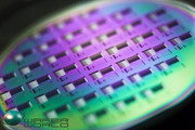
The development process of wafers
Specifically, in present competitive, dynamic semiconductor industry market, producing a sustainable product proves to be crucial and an added advantage as well. The procedure of semiconductor begins with a large ingot a meticulous huge material which is sliced into small sizes of flat layers called as wafers.
Wafers undergo numerous chemical and other sorts of mechanical process that later produced as single chip placed onto the wafer. The effective procedure of life cycle helps to manufacture smart wafer chips.
Comments
Post a Comment